Potting, Conformal Coating, or Nano Coating? A Clear Comparison of Cost, Repairability, and Reliability
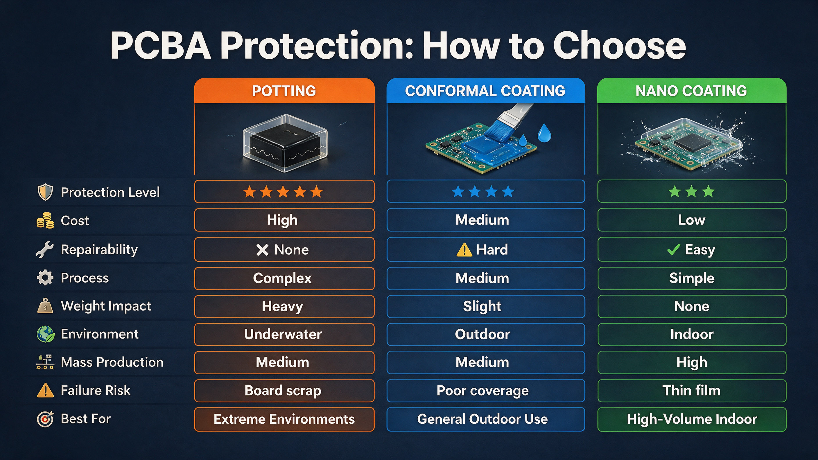
I. The Fundamental Difference: Film Thickness Spans Three Orders of Magnitude
To understand the differences among the three schemes, start with film thickness — the most intuitive indicator that reflects their differing protection philosophies.
Conformal Coating applies a "thin, tough skin" to the PCB surface. Mainstream materials include acrylic, polyurethane, and silicone, with a typical film thickness of 25–75 μm. Acrylic conformal coating is low-cost and easy to rework, suitable for indoor electronics; polyurethane offers better water and abrasion resistance but is difficult to remove; silicone has a wide temperature range and good flexibility, suitable for high-temperature and flexible applications. Conformal coating has been used in the electronics industry for decades, and its greatest advantages are mature processes and a complete supply chain.
Potting puts a "hard shell" around the PCBA. Epoxy resin and silicone are the mainstream potting materials, with film thickness measured in millimeters, typically fully encapsulating the entire board or critical areas. Epoxy potting offers the strongest protection and high hardness but is non-repairable; silicone potting is more flexible, has a wider temperature range, and offers relatively better repairability. Potting is irreplaceable in extreme-environment applications such as power modules and high-voltage devices.
Nano Coating positions itself as an "invisible armor." Depending on the technology route, liquid-phase fluorinated/PFAS-free coatings range from 0.05–10 μm, PECVD (plasma-enhanced chemical vapor deposition) coatings from 0.015–3 μm, and Parylene CVD coatings from 2–25 μm. The most mainstream liquid-phase nano coating is 50 to 1,000 times thinner than conformal coating, completely invisible to the naked eye, yet capable of providing protection ranging from moisture resistance up to IPX7.
In short: from 0.05 μm for nano coating to the millimeter scale for potting, the three schemes span three orders of magnitude in film thickness, corresponding to entirely different protection philosophies — an ultra-thin barrier, a tough skin, or a rigid armor. Understanding this fundamental difference is the first step in selection.
II. Eight-Dimensional Comparison: Which Route Truly Fits Your Product?
Film thickness is only the starting point. Practical selection requires a comprehensive consideration of protection capability, process compatibility, cost, and maintainability. The table below systematically compares the three schemes and their main sub-routes across eight core dimensions.
| Dimension | Acrylic Conformal Coating | Polyurethane Conformal Coating | Silicone Conformal Coating | Epoxy Potting | Silicone Potting | Parylene | Liquid-Phase Nano Coating | PECVD Nano Coating |
|---|---|---|---|---|---|---|---|---|
| Typical Film Thickness | 25–75 μm | 25–75 μm | Thicker | Millimeter scale | Millimeter scale | 2–25 μm | 0.05–10 μm | 0.015–3 μm |
| Protection Capability | Moderate moisture resistance | Good water & abrasion resistance | Wide temp range, flexible | Strongest protection | Flexible, wide temp range | Extremely uniform | Moisture to IPX7 | IPX3–IPX8+ |
| Application Method | Spray / brush | Spray / brush | Spray / potting | Potting | Potting | Vacuum CVD | Dip / spray | Vacuum PECVD |
| Masking Requirement | Extensive masking | Extensive masking | Extensive masking | No masking but requires molds | No masking but requires molds | Contact-point masking required | Low-concentration can be mask-free | Can cover connectors |
| Curing Time | 24 h or bake | Slow | Slow | Long | Medium | Vacuum deposition, hours | Tack-free 2–10 min | 0.5–2 h/batch |
| Reworkability | Easy to rework | Difficult to remove | Repairable | Non-repairable | Relatively good repairability | Generally difficult to rework | Solder-through / alcohol wipe, reworkable | Reworkable |
| Equipment Investment | Low | Low | Low | Low | Low | High | Low–Medium | High |
| Unit Cost | Low | Low–Medium | Medium | Medium (material + molds) | Medium–High | High | Low–Medium | Medium–High |
| Weight / Space | Lightweight | Lightweight | Lightweight | Heavy, space-consuming | Heavy, space-consuming | Extremely light & thin | Extremely light & thin | Extremely light & thin |
| Environmental Compliance | Some contain VOC | Some contain VOC | Some contain VOC | — | Zero VOC | Some contain PFAS / PFAS-free available | Depends on precursor | |
| Typical Applications | Indoor electronics | Automotive / industrial | High-temp / flexible | Power / high-voltage | Flexible / high-temp | Medical / military / aerospace | Consumer electronics / IoT | High-end phones / 5G / hearing aids |
Note: The above parameters are typical ranges for each technology route; specific product performance is subject to the supplier's latest TDS. Cost comparisons are based on typical operating conditions and may vary with product complexity, production volume, and regional differences.
The Value of "Thin": More Than Just Material Savings
Nano coating is 50 to 1,000 times thinner than conformal coating, and this difference is critical in space-sensitive products such as smartphones, TWS earbuds, and smartwatches.
The 25–75 μm film thickness of conformal coating can affect contact reliability and RF signals at connector pins, gold fingers, and antenna areas, necessitating masking. The ultra-thin 0.05–10 μm layer of nano coating — especially low-concentration products — can directly cover connectors and contacts without affecting electrical connections, with contact resistance changes at the μΩ level. For antenna areas, nano coating has a dielectric constant of approximately 3.0 @ 1 kHz, with minimal impact on high-frequency signals such as Bluetooth and Wi-Fi. In terms of thermal management, the ultra-thin coating also impedes PCB heat dissipation far less than thick-film conformal coating and potting layers.
For products like TWS earbuds, where the PCBA area is measured in square centimeters and component density is extremely high, "thin" is not a nice-to-have — it is a hard constraint.
The Hidden Cost of "Rework": Masking Labor and Downtime Losses
Reworkability is the most underrated dimension in selection.
Before applying conformal coating, connectors, gold fingers, test points, and sockets require extensive manual masking — known in the industry as "taping." For a complex smartphone motherboard or industrial control board, masking labor can account for over 60% of the entire coating process. During rework, acrylic conformal coating is relatively easy to remove, but polyurethane conformal coating is extremely difficult, requiring specialized solvents and mechanical abrasion that can easily damage pads and components.
Potting's reworkability is even more extreme — epoxy potting is essentially non-repairable, and once a component fails, the entire PCBA must be scrapped. This is acceptable in scenarios with low in-service repair probability, such as power modules, but in consumer electronics and automotive electronics, after-sales repair costs must be factored into the BOM.
Liquid-phase nano coating has a clear advantage in reworkability: most products are solder-through (the coating decomposes or is penetrated by solder at welding temperatures), and rework simply requires touch-up coating; some products can be directly wiped off with alcohol. The mask-free characteristic of low-concentration products also significantly reduces pre-application labor.
"Total Cost" Rather Than "Material Cost"
A common pitfall in procurement decisions is looking only at material unit price. Conformal coating material cost is indeed low, and nano coating unit price may be higher — but when the following hidden costs are factored in, the conclusion may be entirely different:
- Masking labor cost: Conformal coating requires extensive manual masking of connectors and test points; low-concentration nano coating can be mask-free.
- Curing waiting cost: Conformal coating requires 24 hours of room-temperature curing or an additional baking line; nano coating reaches tack-free in just 2–10 minutes and can seamlessly integrate into SMT lines.
- Rework downtime cost: Conformal coating rework requires coating removal, re-masking, and re-coating; nano coating allows solder-through rework with simple touch-up.
- Yield loss: Uneven thickness, bubbles, and cracks in conformal coating can lead to batch defects; nano coating dip/spray processes offer better consistency.
- Weight and space cost: The added weight of potting cannot be ignored in weight-sensitive products such as drones and wearables.
According to a public DONAT case study, a smart home manufacturer that replaced conformal coating with nano coating saw a 35% reduction in after-sales failure rates and a 22% reduction in per-unit labor costs. In a 5G communications case publicized by P2i, a global telecom customer experienced a 43% reduction in field failures and a 60% reduction in maintenance costs. While these figures come from specific application scenarios, they point to the same conclusion: the true cost of a protection scheme is its "full-lifecycle cost," not the material unit price on the procurement BOM.
III. Three Questions for Selection: A Decision Path Starting from Requirements
The eight-dimensional comparison provides a panoramic view, but practical selection does not require comparing every dimension one by one. Answering the following three questions narrows the scope to a clear set of solution combinations.
Question 1: How Much Protection Does Your PCB Need?
Protection level is the first screening criterion. From indoor moisture resistance to continuous immersion, different environmental threats correspond to different solution choices:
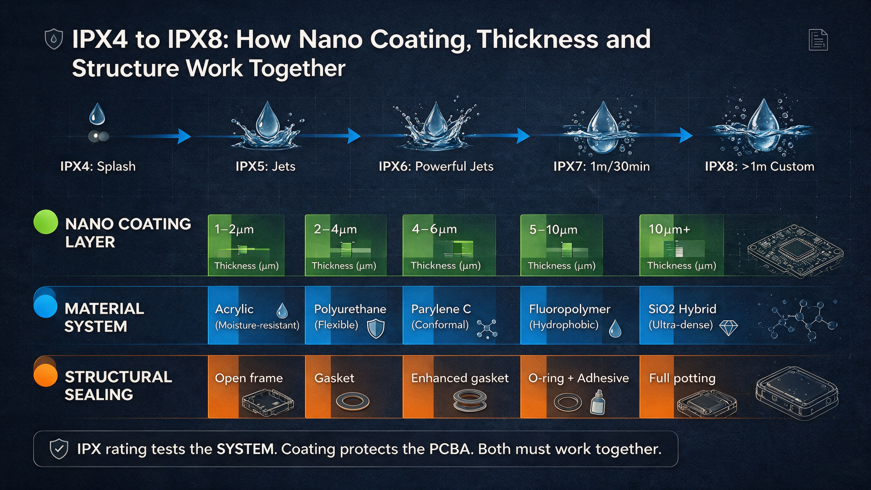
- Moisture / condensation protection (indoor small appliances, ordinary smart hardware) → Nano coating (50–800 nm) or thin conformal coating is sufficient; nano coating offers advantages in application efficiency and reworkability.
- Splash protection / IPX4–IPX5 (earbuds, smart door locks, kitchen & bathroom appliances) → Enhanced nano coating (500–3000 nm) or conformal coating both work; selection should consider space constraints and production cycle time.
- Short-term immersion / IPX7 (wearables, outdoor IoT, handheld devices) → High-waterproof nano coating (2–5 μm) combined with structural sealing, or localized potting of critical areas.
- Continuous immersion / extreme environments (industrial modules, marine equipment, military) → Composite schemes combining PECVD/Parylene with potting and structural waterproofing; a single coating is insufficient.
It is important to emphasize that IP rating is a system-level test result for the entire device, and coating is only one component of the protection scheme. Coating film thickness and performance must be co-designed with enclosure sealing, connector selection, and assembly processes.
Question 2: Do You Need Rework?
Reworkability determines the cost structure of a scheme during the after-sales phase:
- After-sales repair required (consumer electronics, communications equipment, automotive electronics) → Prioritize liquid-phase nano coating (solder-through / alcohol wipe) and acrylic conformal coating (easy to rework); polyurethane conformal coating and Parylene are difficult to rework.
- One-time sealing (power modules, high-voltage devices, certain medical implants) → Potting and Parylene are reasonable choices, as these scenarios are not expected to require rework.
- Partial rework (most industrial and automotive products) → A composite scheme of nano coating + localized potting: full-board nano coating ensures moisture protection and reworkability, while critical device areas receive localized potting for enhanced protection.
Question 3: What Process Can Your Production Line Accept?
Process compatibility determines the implementation cost and mass-production feasibility of a scheme:
- Existing SMT line, limited equipment investment budget → Liquid-phase nano coating (dip/spray) is the most friendly option; tack-free in 2–10 minutes, directly integrable into the production line, no vacuum equipment required.
- Vacuum equipment budget available, 追求 film uniformity → PECVD is suitable for high-end smartphones, hearing aids, 5G base stations, and other scenarios demanding high uniformity and coverage.
- No cost constraints, pursuing maximum reliability → Parylene and ALD offer irreplaceable advantages in medical, aerospace, and military fields, but deposition is slow and costly.
- Products with high-voltage / high-current areas → Potting remains the first choice for insulation and physical protection, and can form a composite scheme with nano coating.
IV. Composite Schemes Are the Norm: Not "Three-Choice-One" but a "Combination Punch"
In high-reliability scenarios, few products use a single protection scheme. The more common approach is to combine multiple protection methods based on the risk level of different PCBA areas.
Typical Combination 1: Nano Coating (Full-Board Moisture Protection) + Localized Potting (High-Voltage / Critical Device Areas)
This is a common scheme in automotive electronics and industrial control. Full-board nano coating provides basic moisture, condensation, and salt spray protection, while critical areas such as power management ICs, high-voltage regions, and BGA chips receive localized epoxy or silicone potting for enhanced protection. This controls the weight and cost penalties of potting while ensuring the reliability of critical devices, and non-potted areas remain reworkable.
Typical Combination 2: Structural Sealing Ring (First Line of Defense) + Nano Coating (Second Line of Defense)
This is the mainstream scheme for consumer electronics and wearables. Enclosure sealing rings and waterproof adhesives prevent most liquid water from entering the housing, while nano coating serves as a "safety net" — ensuring that water entering the housing due to seal aging, assembly gaps, or accidental immersion does not cause PCBA short circuits and corrosion. This "structural waterproofing + board-level coating" dual-layer protection concept has become the design paradigm for IPX7 and higher-rated products.
Typical Combination 3: Conformal Coating (Mature Scheme) + Nano Coating (Edge Connector / Gap Enhancement)
On production lines with existing conformal coating processes, nano coating can be added for edge connectors, fine-pitch IC pins, and micro-gap areas that conformal coating struggles to cover. The excellent penetration and ultra-thin characteristics of nano coating can fill coverage blind spots of conformal coating, while conformal coating provides mature abrasion and insulation protection in the main areas.
Regardless of the combination, the core logic is layered protection: each layer of defense addresses different levels of threat, and the failure of a single layer does not lead to systemic collapse. This design approach is more pragmatic and reliable than pursuing "one material to solve all problems."
V. Compliance Trends: A Variable That Cannot Be Ignored in Selection
Protection scheme selection is not only a technical decision but also a compliance decision. The following three trends are influencing coating choices across the global electronics supply chain:
The impact of PFAS regulation on fluorinated nano coatings. The EU REACH PFAS restriction proposal covers over 10,000 PFAS substances, with a general ban expected to take effect as early as 2028–2029. Fluorinated polymer nano coatings currently account for approximately 61.9% of the global PCB nano coating market (according to a 2026 pmarketresearch report), and the electronics and semiconductor industry has been listed by SEAC as a "technical challenge" sector, potentially receiving a 5-year or longer exemption — but the long-term direction toward substitution is clear. Products exported to Europe and the US should prioritize evaluating PFAS-free nano coating solutions. According to public ViriDyn product data, its PFAS-free coating 101-XP-300 has a film thickness of 0.5–1.0 μm, water contact angle >100°, dielectric constant 3.0 @ 1 kHz, breakdown strength 3000 V/mil, fast curing in 5–30 seconds, and solder-through reworkability — with core indicators already approaching fluorinated systems.
The VOC issue in conformal coating. Acrylic and some polyurethane conformal coatings contain volatile organic compounds (VOCs), facing pressure amid tightening environmental regulations and rising workplace air quality requirements. Low-VOC / VOC-free formulations and water-based conformal coatings are the development direction, but currently involve trade-offs in performance and process compatibility.
Environmental disposal of potting materials. Epoxy potting bodies are difficult to recycle and do not align with circular economy trends. Amid tightening EU WEEE directives and national e-waste regulations, repairable and disassemblable protection schemes are more sustainable in the long run.
For companies supplying both domestic and overseas markets, it is recommended to add a "compliance foresight" dimension to protection scheme selection: not only assessing whether the current scheme meets performance requirements, but also evaluating the impact of regulatory changes over the next 3–5 years on the supply chain.
Conclusion
Potting, conformal coating, and nano coating are not mutually exclusive competitors — they are protection methods each with their own applicable boundaries. Potting's physical protection in extreme environments is irreplaceable; conformal coating's mature processes and low cost still have extensive application scenarios; and nano coating's ultra-thin profile, fast curing, reworkability, and mask-free characteristics demonstrate clear comprehensive cost advantages in consumer electronics and IoT.
From IPX4 to IPX8: How Nano Coating Thickness, Material Systems, and Structural Waterproofing Work Together
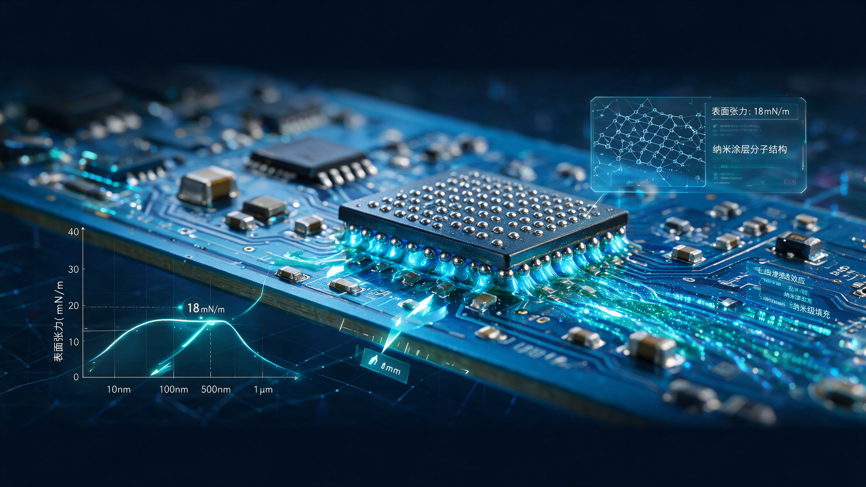
Surface Tension as Low as 18 mN/m — Full Analysis of Nano‑Coating "Capillary Penetration" Technology
Related Article